
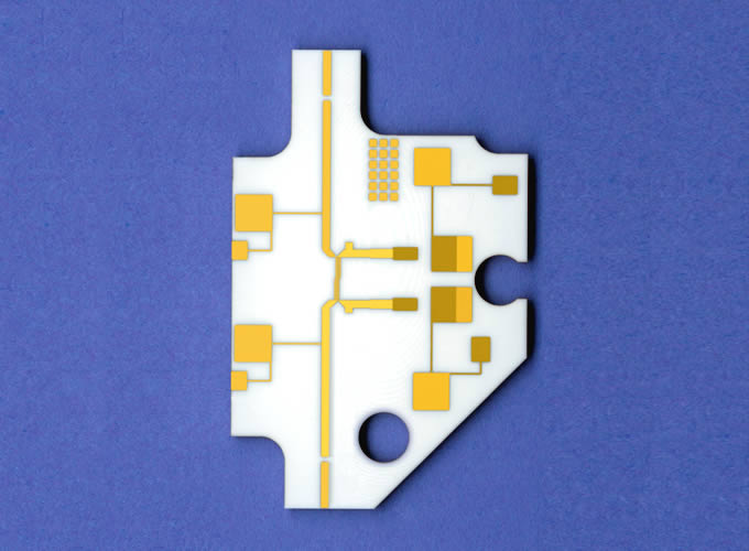


Thin film microcircuits
LEW Techniques’ dedicated thin film manufacturing capability offers a build-to-print service for high performance microcircuits on a wide range of materials. From simple single layer interconnects to multilayer, double-sided circuits with fine lines, integrated resistors, inductors, metallised vias and complex substrate profiles, our manufacturing know-how and dedicated in-house facilities allow us to offer a comprehensive and versatile service for demanding applications.
Capability outline
Substrates
Standard substrate materials include:
Metallisations
| Typical metallisation schemes include: | |
|---|---|
| TiW/Au | For epoxy assembly and AuSn soldering |
| TiW/Pd/Au | For SnPb, SnAg soldering |
| TiW/Pd/Au/Ni/Au | For additional soldering leach resistance |
| Ti/Pt/Au | Best soldering performance but more costly |
| NiCr or TaN | For integrated resistors |
| Patterning |
|---|
| Utilising wet or dry film, positive and negative photo resists and high accuracy mask alignment, fine high density lines and features are resolved to create the desired circuit. |
| Line widths | Typical | High spec. |
|---|---|---|
| Minimum line width | 25 µm | 10 µm |
| Minimum gap width | 25 µm | 10 µm |
| Line/gap tolerance | ±10 µm | ±3 µm |
| Line to feature (e.g. hole) | ±50 µm | ±25 µm |
| Resistors |
|---|
| Integrated resistors are formed using NiCr or TaN seed layers which are exposed where desired and may be laser trimmed to precise values. |
| Multilayers |
|---|
| Crossovers, air bridges and multilayer circuits can be realised using photo-imagable polyimide as an insulating layer. |
| Vias |
|---|
| Plated thru holes or filled vias can be incorporated to provide localised grounding or front-to-backside connections. |
Laser machining
Intricate profiles, pockets, notches and vias can be formed in the substrate before or after metallising. Alignment features, serial numbers and solder dams can also be marked onto the substrate or metallised surfaces.
Pre-deposited AuSn
AuSn solder can be selectively pre-deposited onto the conductors. This removes the need to use a solder preform. Alignment, thickness and alloy control are dependent upon the underlying conductor metallisation and component geometry.
Singulation
Individual circuits can be singulated from the substrate by laser profiling or by scribe and snap. For best edge quality diamond sawing is the preferred method.
Data format
Designs can be handled in DWG, DXF, GDSII or Gerber format, or as hard copy drawings or
sketches.
Click here to download a copy of our thin film microcircuits design guidelines.