


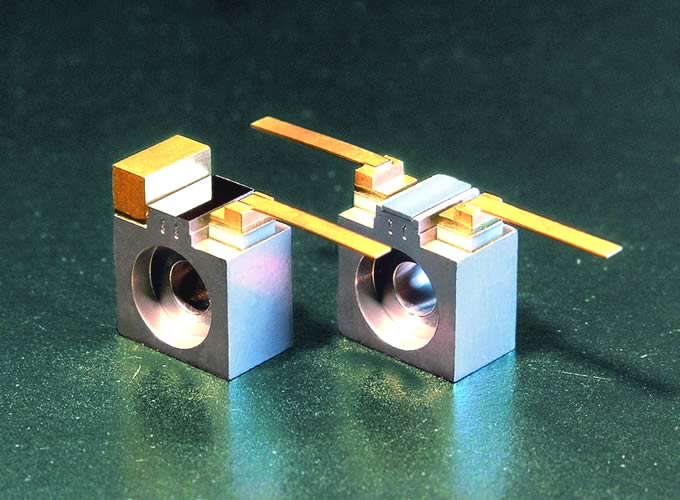


Thin film coating
LEW Techniques offers a subcontract service for the vacuum coating of components with thin films. For demanding applications thin films of metals can be sputtered or evaporated onto metals, ceramics, or other difficult-to-coat surfaces. These coatings can provide conductive and solderable layers on non-conductive materials or barriers and protective finishes on difficult-to-plate metals. Our manufacturing know-how and dedicated in-house facilities allows us to offer a comprehensive and versatile service.
Capability outline
Applications
Facilities
Housed in a class 10,000 clean room, our thin film facilities include:
Complementary capabilities
Component materials
Component geometry limits
Coatings
Depending on the equipment and coating types required up to four different coatings can be sequentially deposited in each coating run.
| Adhesion | Ti, Cr, NiCr, TiW, TaN |
| Barrier | Pd, Pt, Ni |
| Conductor | Cu, Au |
| Solder | AuSn |
| Typical coating schemes include: | |
|---|---|
| Cr/Au | For decorative/reflective finish |
| TiW/Pd/Au | For SnPb, SnAg soldering |
| TiW/Pd/Au/Ni/Au | For additional soldering leach resistance |
| Ti/Pt/Au | Best soldering performance but more costly |
| NiCr | For protective finish |
| Ti/Cu/Ni/Au | For high conductivity |
| AuSn | Solder pre-deposition for critical attach |
| Typical deposition thickness: | |
| Adhesion layers | 100 – 2000 Å (angstroms) |
| Barrier layers | 0.1 – 2 μm |
| Conductors | 0.2 – 5 μm |
Masking
By using physical masks the coatings can be selectively deposited onto required areas only.
High resolution patterning
Utilising wet or dry film photo resists, fine high density lines and features can be resolved to create circuits, logos and other images.
Microcircuits
Contact us for details of our comprehensive capabilities for manufacturing RF and optoelectronic microcircuits.