


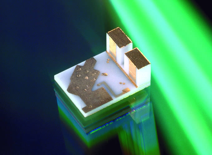
Photodiode mounts/carriers
Metallised ceramic mounting blocks with optional wrap around conductors for mounting of photodiodes. This type of mount is often used as a BFM (back facet monitor) for laser diodes and for other sensing applications.
Ceramic material
The ceramic substrate material is typically alumina (90%, 96% or >99%).
Mechanical dimensions
| Diamond sawing: | Min. | Max. | Typ. tol. | Tight tol. |
|---|---|---|---|---|
| Length and width | 1.0 x 1.0 mm | 75 x 10 mm | ±0.05 mm | ±0.020 mm |
| Thickness | 0.125 mm | 2.0 mm | ±0.05 mm | ±0.010 mm |
| Pattern to edge gap | 0.025 mm | n/a | ±0.05 mm | ±0.025 mm |
| Laser profiling: | ||||
| Hole diameter | 0.15 mm | n/a | ±0.05 mm | ±0.025 mm |
| Hole to hole | = thickness | n/a | ±0.05 mm | ±0.025 mm |
| Pattern to edge gap | n/a | n/a | ±0.05 mm | ±0.025 mm |
Machined features
Slots, grooves, angles, holes, apertures, cut outs, chamfers, etc. can all be realized by precision diamond machining or laser drilling or profiling.
Moulded features
For special applications the ceramic body can be moulded and fired to shape before metallising, allowing for complex shapes not economically realizable by
machining.
Thick film metallisations
For lowest cost, thick film metallisations are screen printed with the required pattern directly onto the ceramics and then fired, usually in air at >800°C, to fix the metal to the ceramic. Special attention is paid to ensure a high reliability of connection where the conductors wrap over the edges of the ceramics.
| Thick Film Type | |
|---|---|
| Au (standard) | Au wire bondable, epoxy attach or AuSn solderable. The most common metallisation system. |
| Au (special) | Modified Au metallisation with excellent flux-free AuSn solderability (see flux-free AuSn solderability). |
| Pt/Au | Platinum doped to improve leach resistance to PbSn and SnAg type solders. Au wirebondable. |
| Pt/Pd/Ag | Doped silver based metallisation for lowest cost. Solderable with fluxed solders. Not wirebondable. |
The thick film metallisation schemes can be mixed on the same or adjoining faces to accommodate varied bonding and soldering processes.
Thin film metallisations
For special applications wrap around conductors can be achieved using thin film type metallisations. Thin films are generally smoother, flatter and better defined than thick films but are usually more costly.
| Thin Film Type | |
|---|---|
| TiW/Pd/Au | Au wire bondable, epoxy attach or solderable. |
| Ti/Pt/Au | Best soldering performance but more costly. |
| Patterning | ||||
|---|---|---|---|---|
| THICK FILM | THIN FILM | |||
| Typical | High spec. | Typical | High spec. | |
| Minimum line width | 150µm | 50µm | 25 µm* | 10 µm* |
| Minimum gap width | 150µm | 50µm | 25 µm* | 10 µm* |
| Line tolerance | ±50µm | ±25µm | ±20 µm* | ±5 µm* |
| Line to feature (e.g. hole) tolerance | ±50µm | ±25µm | ±50 µm* | ±25 µm* |
Alignment guides/fiducials can be incorporated into design for subsequent automated assembly.*
*Dependent upon imaging method available (design dependent).
Flux-free AuSn soldering – thick and thin film
Thin film materials usually provide very good surfaces for flux-free AuSn soldering. Obtaining good results using traditional thick film metallisations normally requires additional processing, but LEW Techniques offers a thick film Au that has exceptionally good flux-free wettability with AuSn. This provides the wettability performance of thin film with the cost benefits of thick film.
Pre-deposited AuSn
For some applications it is possible to selectively pre-deposit AuSn solder onto the conductors. This removes the need to use a solder preform. Alignment, thickness and alloy control are dependent upon the underlying conductor metallisation and component geometry.
Angled photodiode mounts
It is possible to produce conductors on an angled face to allow the photodiode to be located close to the rear facet of a laser diode without causing emitted light to be reflected back into the laser. This can reduce the real estate required and aid miniaturisation.
Assemblies
Metallised ceramics can be assembled to other ceramics or metal components to produce precision assemblies. Joints can be realized by several means, including soldering and glassing.
For further details please contact us for datasheets about our thick and thin film microcircuit manufacturing capabilities, design guidelines and materials specifications, or find them on this website.